Every VLSI engineer knows that standard cells need power. But how does power actually travel from the package bumps at the top of the chip all the way down to the M1 VDD/VSS rails inside individual standard cells? And what happens when the chip has multiple voltage domains that must remain electrically isolated?
This article walks through the physical power distribution hierarchy in a multi-voltage SoC — from package supply through upper-metal meshes, block straps, via stacks, and local cell rails. We cover UPF power intent vs. physical implementation, explain why designers keep dense PG routing off lower metals, and show exactly how a dual-rail level shifter gets its two supplies. If you are preparing for interviews at Google, Apple, Qualcomm, NVIDIA, AMD, or any semiconductor company, this is the material you need to internalize.
Power Domain vs. Voltage Area
The important distinction is:
- Power Domain — a logical group of design elements sharing a power policy and primary supply. Defined in UPF.
- Voltage Area — the physical floorplan region where cells belonging to that power domain are placed.
For our teaching example:
PD_CPU  = CPU logic, 0.8 V    (switchable — can be powered down)
PD_AON  = Always-on logic, 1.0 V  (never powered down)
The voltage area defines where the physical-design tool is allowed to place cells from each domain. Cells from PD_CPU live inside the CPU voltage area; cells from PD_AON live inside the AON voltage area. The power networks within each region are electrically separate.
UPF Power Intent vs. Physical Power Grid
Do not confuse the logical power intent specification (UPF) with the physical metal that carries current. They serve different purposes:
UPF Describes Intent
create_power_domain PD_CPU -elements {cpu_core}
create_power_domain PD_AON -elements {aon_ctrl pmu}

create_supply_port VDD_CPU_PORT
create_supply_port VDD_AON_PORT
create_supply_port VSS_PORT

create_supply_net VDD_CPU -domain PD_CPU
create_supply_net VDD_AON -domain PD_AON
create_supply_net VSS

connect_supply_net VDD_CPU -ports {VDD_CPU_PORT}
connect_supply_net VDD_AON -ports {VDD_AON_PORT}
connect_supply_net VSS     -ports {VSS_PORT}

set_domain_supply_net PD_CPU \
    -primary_power_net VDD_CPU \
    -primary_ground_net VSS

set_domain_supply_net PD_AON \
    -primary_power_net VDD_AON \
    -primary_ground_net VSS
connect_supply_net means "explicitly connect a logical supply net to supply ports or pins." set_domain_supply_net means "define which supply nets are the default primary power and ground for normal logic in that power domain." Neither command draws metal.
Exact UPF syntax can vary by UPF revision and EDA tool. The example is for conceptual learning.
Physical Implementation Creates Metal
Physical design operations that actually build the power grid:
- Creating upper-metal power meshes
- Creating block-level power straps
- Creating standard-cell M1 rails
- Creating via stacks connecting mesh to rails
- Connecting PG pins of special cells
- Running IR-drop analysis
- Running electromigration (EM) analysis
From Package Bump to Standard Cell
Power travels through a well-defined hierarchy. Here is the path from external supply to transistor:
Package / C4 bump / micro-bump
        ↓
Upper-metal global power mesh (M9/M10)
        ↓
Block-level power mesh / straps (M7/M8)
        ↓
Intermediate straps (M5/M6)
        ↓
Via arrays / stacked vias
        ↓
Lower/local power strap (M3/M4)
        ↓
M1 standard-cell power rail (VDD/VSS)
        ↓
Standard-cell VDD/VSS pin
        ↓
Internal library routing
        ↓
Transistors
The critical principle:
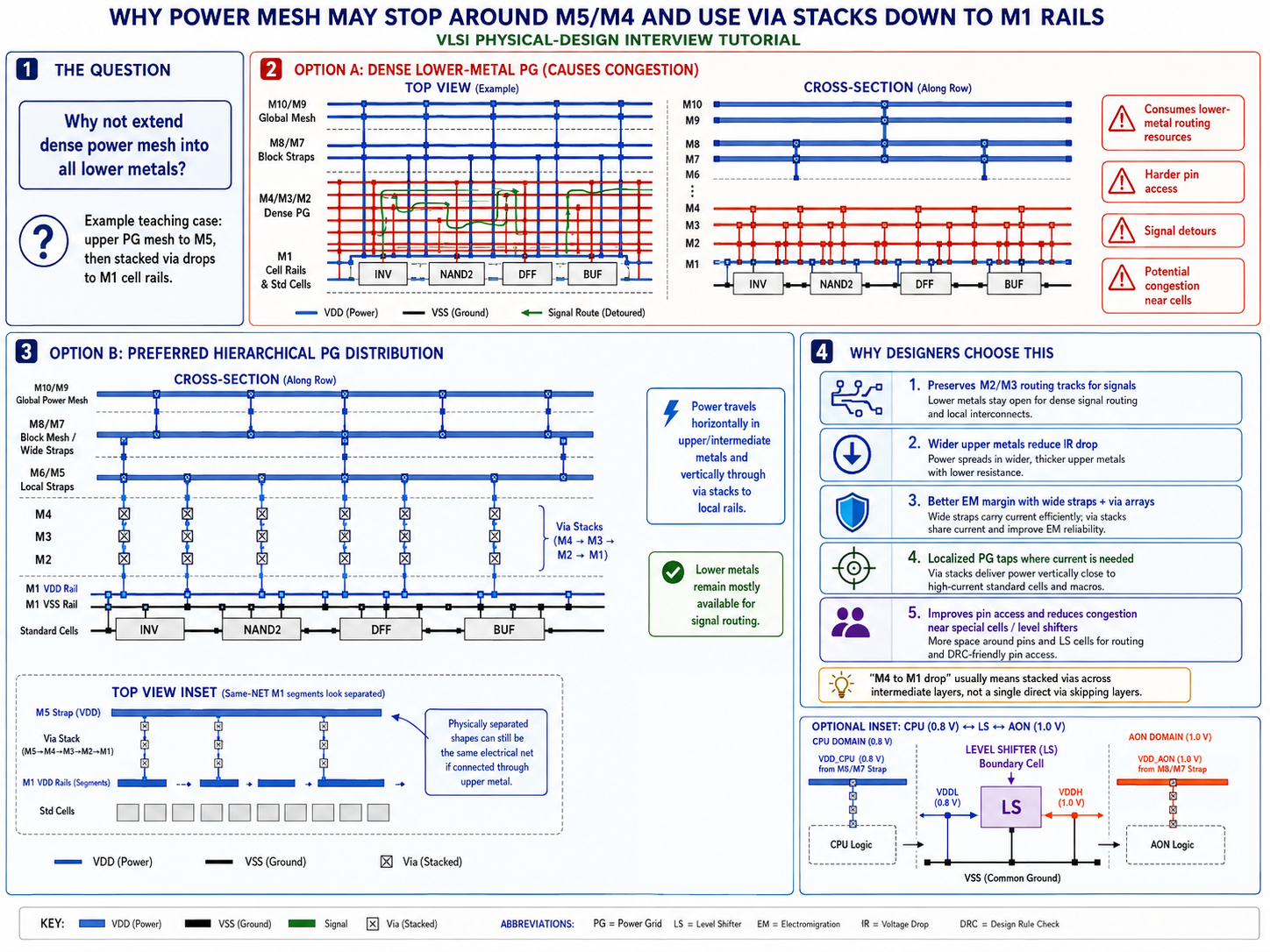
Power travels horizontally through metal and vertically through vias.
Why Multiple Vias?
Via stacks use many parallel vias (via arrays) for critical reasons:
- Lower resistance — parallel paths reduce total R
- Higher current capability — current is shared across vias
- Better electromigration reliability — current density per via is lower
- Reduced voltage drop —
Vdrop = I × R
For interviews, remember these two equations:
V_drop = I × R     (voltage drop across resistance)
J = I / Area       (current density — EM limit)
Are Power Rails Continuous or Broken?
Same Electrical Net — Can Look Broken
A local M1 rail can appear physically segmented:
====== VDD_CPU =====     ===== VDD_CPU =====
                    (gap on M1)
But both segments can still be electrically connected through an upper-metal strap:
        |                     |
       via                   via
        |                     |

========================================
             M5 VDD_CPU strap
========================================
Physical continuity on one layer is NOT required for electrical continuity of the entire PG network. Segments on the same net are connected somewhere in the metal hierarchy.
Different Electrical Nets — Must Stay Isolated
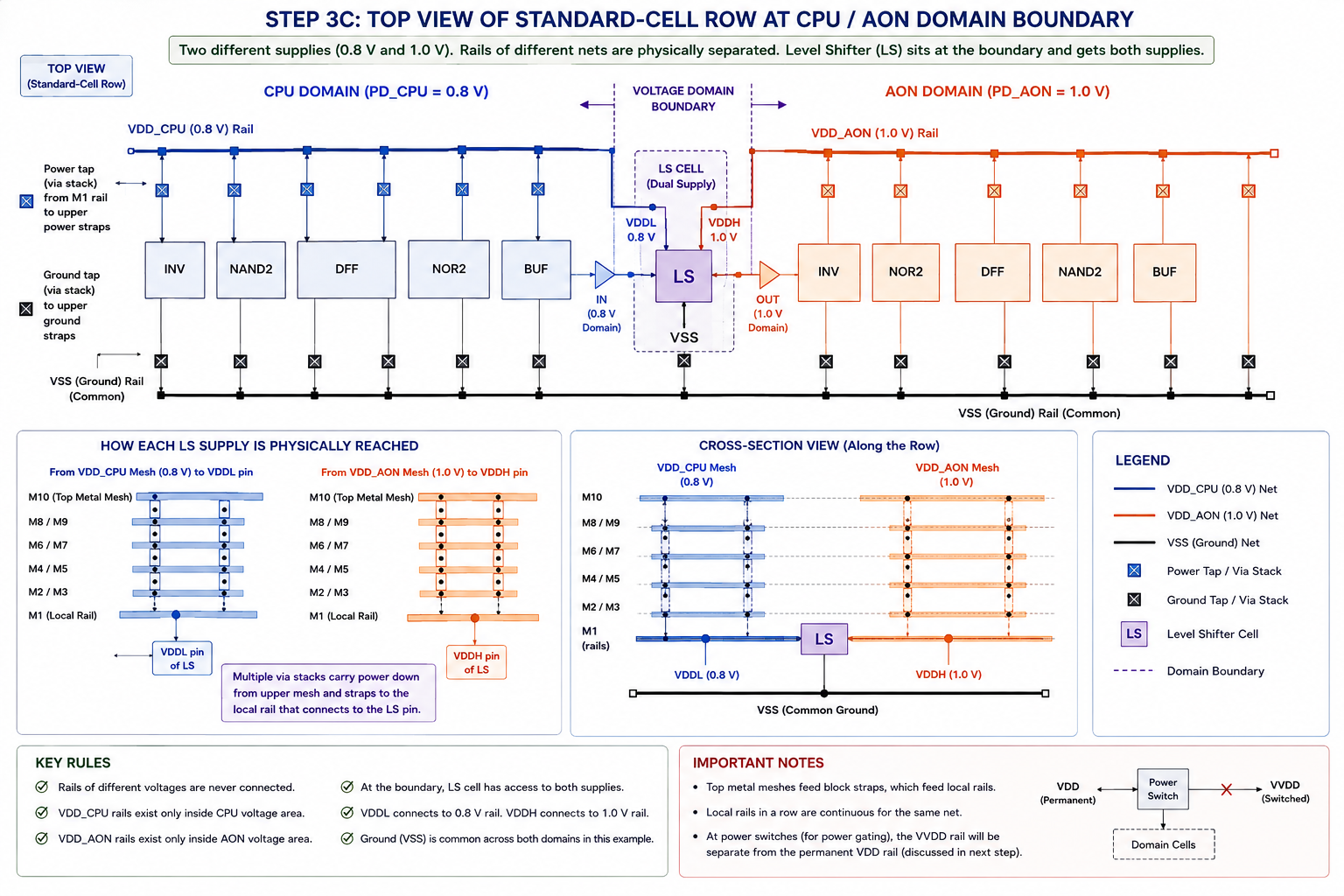
Supplies belonging to different voltage domains must remain physically isolated:
VDD_CPU = 0.8 V    ← separate electrical network
VDD_AON = 1.0 V    ← separate electrical network

These NEVER connect to each other. Only signals cross between
domains — through level shifters.
Why the Dense Power Mesh Often Stops on Intermediate Metals
There is nothing universal about M4 or M5 as the "drop layer." The exact choice depends on process technology, number of routing layers, preferred routing direction, standard-cell library, IR-drop targets, EM targets, congestion, macro placement, power density, foundry rules, and EDA methodology.
However, a common conceptual architecture looks like:
M10/M9  — Global PG mesh (widest straps, lowest R)
M8/M7   — Block PG straps
M6/M5   — Local/block PG mesh
M4      — Power drop / tap layer

        ↓ stacked vias (M4→V3→M3→V2→M2→V1→M1)

M1      — Standard-cell power rail
Physically, "M4 directly to M1" means:
M4
 ↓ Via3
M3
 ↓ Via2
M2
 ↓ Via1
M1
It does NOT mean a single via that skips intermediate layers. There may simply be little or no long horizontal PG routing on M2/M3 — those layers pass through vertically via short landing pads.
Why Keep Dense PG Off Lower Metals
1. Preserve Lower-Metal Routing Resources
M1, M2, and M3 are critically important for:
- Local signal routing
- Standard-cell pin access
- Clock tree routing
- ECO connections
- Short timing-critical nets
Dense PG routing on these layers causes congestion, signal detours, pin-access failures, DRC violations, increased capacitance, and timing degradation.
2. Lower Resistance in Upper Metals
Upper metals can support wider, thicker conductors — meaning lower sheet resistance per square. A wide upper-metal strap carrying current horizontally plus a short vertical via-stack drop is far more efficient than running long thin power routes on M2/M3.
3. Better Electromigration Margin
Large current in narrow wires or too few vias increases current density (J = I / Area). Upper metals allow wider straps, parallel current paths, multiple via arrays, and distributed PG taps — all improving EM reliability.
4. Better Standard-Cell Pin Access
          signal pins
        A B CLK D Q

      +-----------+
      |    DFF    |
      +-----------+

VDD =================
VSS =================
Filling M2/M3 with dense power straps makes it difficult for the router to reach signal pins from above. Pin access is one of the most congestion-sensitive metrics at advanced nodes.
5. Standard-Cell Library Constraints
The library already defines VDD/VSS rail locations, PG pin shapes, signal-pin access points, and legal metal layers. Do not assume all PG pins are always on M1 — VDDL, VDDH, VDD, VSS and other PG pins are defined by the physical library / LEF and may be exposed on different supported layers.
How a Dual-Rail Level Shifter Is Powered
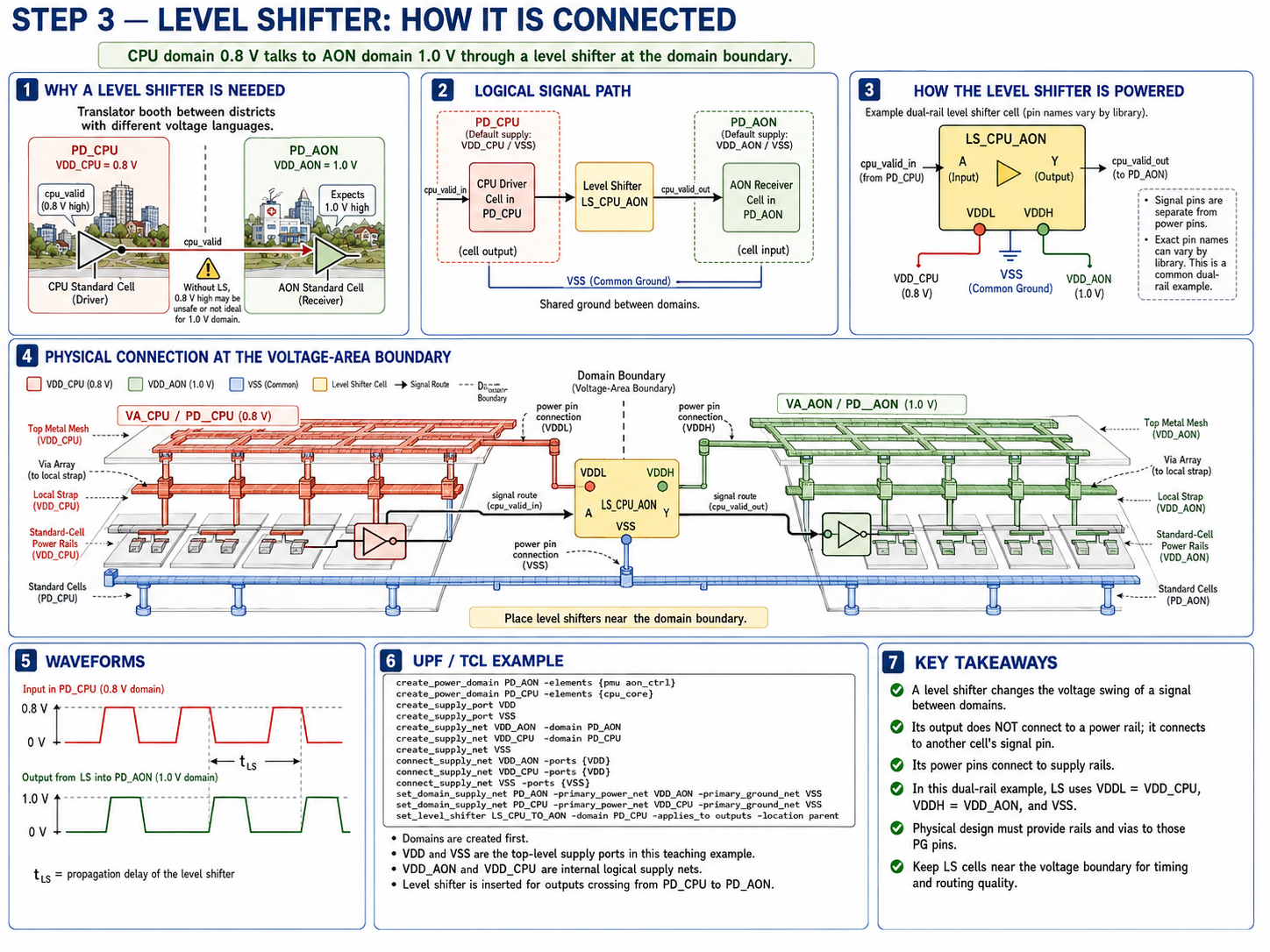
When a signal crosses from a low-voltage domain to a high-voltage domain, a level shifter translates the voltage swing. Think of it as the "translator booth" between two districts that speak different voltage languages.
For our example:
PD_CPU  = 0.8 V  (source domain)
PD_AON  = 1.0 V  (destination domain)
Logical Signal Path
CPU/Q → LS/A → LS internal translation → LS/Y → AON/DPower Path for a Dual-Rail Level Shifter
VDD_CPU (0.8 V) → LS/VDDL   (low-voltage supply pin)
VDD_AON (1.0 V) → LS/VDDH   (high-voltage supply pin)
VSS             → LS/VSS    (common ground)
The critical distinction that interviewers test:
The level shifter output is a signal net. It does NOT connect to the destination power rail. Instead, the destination power rail powers the level shifter output stage so that its signal can swing to the destination-domain voltage.
Level-Shifter Signal Path vs. Power Path
                 VDD_CPU upper mesh
                        |
                      vias
                        |
                 VDD_CPU local strap
                        |
                      VDDL
                         \
                          \
CPU/Q ──────────────────→ [ LEVEL SHIFTER ] ──────────────────→ AON/D
                          /
                         /
                      VDDH
                        |
                 VDD_AON local strap
                        |
                      vias
                        |
                 VDD_AON upper mesh

                          |
                         VSS
                          |
                 common ground network
Physically, this means:
- The level shifter sits at or near the voltage area boundary
- It must be reached by both VDD_CPU and VDD_AON power networks
- The physical-design tool extends straps from both domains to the LS PG pins
- The PG pin locations and layers are defined by the library/LEF
Level-Shifter Waveforms and STA Impact
CPU domain / LS input (0.8V swing):

0.8V       ┌───────┐
           │       │
0V   ──────┘       └────────────


LS output / AON domain input (1.0V swing):

1.0V            ┌───────┐
                │       │
0V   ───────────┘       └────────
            ← tLS →
Key points for STA:
- Logic information stays the same — a 1 is still a 1
- Electrical voltage swing changes — 0.8V → 1.0V
- The level shifter adds propagation delay (tLS)
- STA must account for this delay on cross-domain paths
- Long unbuffered routes before the LS hurt timing — keep LS cells close to the domain boundary
UPF Level-Shifter Strategy
set_level_shifter LS_CPU_TO_AON \
    -domain PD_CPU \
    -applies_to outputs \
    -rule low_to_high \
    -location fanout
This tells the synthesis/implementation tool: "For all output signals leaving PD_CPU that go to a higher-voltage domain, insert a level shifter, and place it in the fanout (destination) domain." Exact options and location semantics depend on UPF version, synthesis implementation, library mapping, and EDA tool.
IR Drop and Electromigration
IR Drop
Every resistive element between the package bump and the cell rail causes voltage drop:
V_cell = V_bump - (I × R_mesh) - (I × R_strap) - (I × R_via_stack) - (I × R_rail)If Vcell drops below the minimum operating voltage, the cell slows down (timing failure) or the logic corrupts (functional failure). Power grid design is fundamentally about keeping IR drop within budget across all operating conditions.
Electromigration
Current flowing through metal causes atomic migration over time. If current density exceeds the EM limit:
J = I / (width × thickness)

If J > J_max → wire degrades over time → open circuit failure
Solutions: wider straps, more vias in parallel, distributed tap points, and keeping high-current PG paths on thicker upper metals.
Common Misconceptions
| Wrong | Correct |
|---|---|
| "Every chip only has one VDD and one VSS port." | Real chips can have multiple independent package supply rails and bump groups. |
| "VDD_CPU and VDD_AON are just names for the same metal." | They represent different electrical networks and can operate at different voltages. |
| "A level shifter output connects to the destination VDD rail." | The LS output is a signal net; its PG pins connect to supply rails. |
| "VDDL and VDDH are always M1." | Physical PG pin layers are library/LEF dependent. |
| "M4-to-M1 power drop means a single via jumps from M4 to M1." | It uses legal stacked via transitions through intermediate layers (M4→V3→M3→V2→M2→V1→M1). |
| "If an M1 rail has a physical gap, the power net is broken." | Separate M1 segments may still be electrically connected through upper-metal PG straps. |
Physical-Design Interview Questions
Q: Why not route the power mesh on every metal layer?
We normally keep large-current long-distance PG distribution on wider upper or intermediate metals, then use distributed via stacks to reach local cell rails. This preserves scarce lower-metal routing resources and pin access, reduces local congestion, improves IR drop and EM reliability, and allows power-entry density to be tuned based on rail analysis.
Q: Does M4-to-M1 mean one via skips M3 and M2?
No. It normally means a stacked via connection through the legal intermediate layer transitions — for example M4–V3–M3–V2–M2–V1–M1 — without necessarily using M2/M3 for long horizontal PG straps. The intermediate layers just have short landing pads for via connectivity.
Q: Can VDD_CPU and VDD_AON touch?
No — if they are different electrical supply nets operating at different voltages, they must remain isolated. Only signals cross between domains through appropriate interface cells such as level shifters.
Q: Can two separate M1 VDD_CPU rail segments still be the same net?
Yes. They can be electrically connected through upper-metal straps and via stacks even if they are not physically continuous on M1.
Q: Where do VDDL and VDDH physically connect on a level shifter?
The PG pin locations and layers are defined by the library/LEF. Physical design connects the required source- and destination-domain supply networks to those PG pins using legal power straps, rails, and via structures.
Q: What is the difference between a power domain and a voltage area?
A power domain is a logical grouping (UPF) — elements sharing a supply policy. A voltage area is the physical floorplan region where those elements are placed. One defines intent, the other defines geometry.
Key Takeaways
- A chip power grid is a hierarchy — not one giant continuous sheet of metal
- Upper metals carry large current efficiently; via stacks bring power down to cell rails
- Shapes on the same supply net are electrically connected somewhere in the hierarchy — physical gaps on one layer don't mean broken connections
- Supplies belonging to different voltage domains must remain isolated
- UPF defines logical intent; physical implementation creates the actual metal
- Lower metals (M1-M3) are preserved for signal routing and pin access
- Level shifters receive both VDDL and VDDH — their output is a signal, not a power connection
- IR drop and EM are the key physical constraints that drive power-grid architecture decisions
A chip power grid is not one giant continuous sheet of metal. It is a hierarchy of connected metal shapes, straps, local rails and via arrays. Shapes belonging to the same supply net are electrically connected somewhere in that hierarchy, while supplies belonging to different voltage domains remain isolated. Upper metals carry large current efficiently, localized via stacks bring power down to cell rails, and special interface cells such as dual-rail level shifters receive the supplies they need while keeping the signal path electrically separate from the power path.
Next Topic: Power Gating, VVDD and Header Switches
Everything above assumes the power supply is always on. But what happens when you want to turn off an entire block to eliminate leakage?
Permanent VDD (always-on rail)
     |
     |
[ HEADER POWER SWITCH ]
     |
     |
VVDD / virtual VDD (switched rail)
     |
     |
CPU standard cells
Here, VDD is the permanent supply and VVDD is the switched/virtual supply. They are separate nets connected only through the power-switch network. This creates additional IR-drop from switch on-resistance, inrush-current during wake-up, wake-up latency, EM concerns through switch cells, and power-sequencing complexity.
We cover this in detail in our Low Power VLSI Design Challenges article.