Power is the constraint that defines modern SoC design. Not area, not timing — power. Every mobile SoC, every IoT edge device, every data center accelerator is fundamentally limited by how much energy it can consume and how much heat it can dissipate. At 7nm and 5nm, power management is not an afterthought you bolt on after timing closure — it is an architectural decision that shapes every stage of the design flow from RTL through GDSII.
This post documents the low-power challenges we encounter on real tapeouts and the techniques that deliver measurable results. These are not theoretical exercises — they are battle-tested methods from production silicon.
Why Low Power Matters More Than Ever
The power equation in CMOS is deceptively simple:
Ptotal = Pdynamic + Pleakage + Pshort-circuit
Where Pdynamic = α · CL · VDD2 · f, and Pleakage = Ileak · VDD. At advanced nodes, both components have exploded for different reasons:
- Mobile and IoT battery constraints — a smartphone SoC has a thermal budget of 3-5W sustained. An IoT sensor must run for years on a coin cell. Every milliwatt counts.
- Data center power budgets — a hyperscale data center spends 40-60% of operating cost on power and cooling. A 10% power reduction across a fleet saves millions annually.
- Thermal density at advanced nodes — at 5nm with 100M+ transistors per mm2, local power density can exceed 100 W/cm2. Thermal runaway is a real threat without aggressive power management.
- Leakage explosion — sub-threshold leakage increases exponentially as threshold voltage (Vt) decreases. At 7nm, leakage can be 30-50% of total power in always-on logic.
- Gate leakage — thin gate oxides at advanced nodes allow quantum tunneling current. FinFET partially mitigates this but does not eliminate it.
The net result: you cannot simply shrink to a new node and get free power reduction anymore. Dennard scaling died at 130nm. Active power management is now mandatory at every level of the design hierarchy.
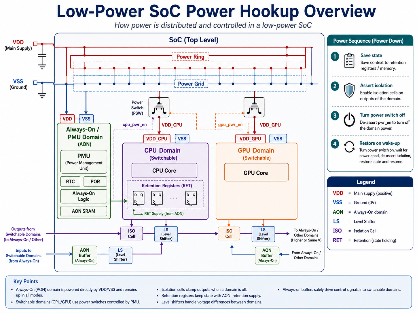
The Eight Key Challenges
1. Leakage Power Explosion at Advanced Nodes
At 7nm and 5nm, sub-threshold leakage dominates idle power. A block that consumes 50mW when active might leak 15-20mW when idle — with no switching at all. Gate leakage adds another 5-10% on top. For SoCs with many always-on domains (always-on controllers, retention logic, power management units), this leakage accumulates rapidly.
The challenge compounds because designers need fast transistors (low Vt) for timing-critical paths, but these same transistors leak orders of magnitude more than high-Vt alternatives. Finding the optimal Vt mix is a multi-dimensional optimization problem.
2. Dynamic Power from High Clock Frequencies
A 2GHz ARM core at 5nm has billions of transistors switching every cycle. Even with low supply voltage (0.75V typical), the aggregate switching capacitance drives dynamic power into the multi-watt range. Clock distribution alone accounts for 30-40% of total dynamic power — the clock tree switches every cycle by definition, regardless of data activity.
3. Multi-Voltage Domain Complexity
Modern SoCs run 5-15 voltage domains simultaneously. Each domain boundary requires level shifters (LS), isolation cells, and always-on logic. The design complexity grows quadratically with domain count: each domain-to-domain interface needs its own set of boundary cells, power sequencing constraints, and verification scenarios.
4. Power Gating Implementation
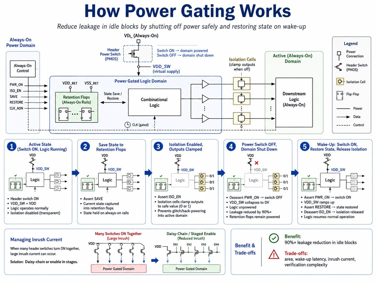
Shutting down unused blocks sounds simple. In practice, power gating introduces rush current (inrush when domain powers up), retention requirements (state must survive shutdown), wakeup latency (time to restore operation), and isolation integrity (outputs must not float during shutdown). Getting any of these wrong results in functional failure or silicon damage.
5. Clock Tree Power Dominance
The clock network is the single largest dynamic power consumer. At 1GHz+ frequencies, the clock tree — buffers, inverters, and wiring — can burn 30-40% of total chip dynamic power. Traditional balanced H-trees and mesh structures prioritize skew minimization but are power-hungry by design.
6. IR Drop Under Worst-Case Switching
When many gates switch simultaneously (worst-case vectors, scan shift), the resulting current surge causes IR drop across the power grid. At 5nm with VDD of 0.75V, even 50mV of IR drop is a 6.7% voltage reduction — enough to cause timing violations. Power grid design must handle peak current without excessive metal overhead.
7. Timing Closure with Multi-Voltage and Multi-Vt
Level shifters add delay. High-Vt cells are slower. Voltage scaling reduces speed quadratically. Every power optimization technique impacts timing. Closing timing while meeting power targets is a multi-objective optimization where gains in one dimension often come at the cost of the other.
8. Verification Complexity
UPF/CPF correctness must be verified across all power states: active, retention, shutdown, and every transition between them. A missing isolation cell causes bus corruption. An incorrect retention strategy loses state. A wrong power sequence damages the chip. Power-aware verification is as complex as functional verification.
Solutions: The Techniques That Work
1. Multi-Vt Cell Swapping
The most impactful leakage reduction technique with zero architectural change. The strategy: start with all HVT cells (lowest leakage), then selectively swap timing-critical paths to SVT or LVT only where needed to meet frequency targets.
- HVT (High Threshold) — 10x lower leakage than LVT, but 20-30% slower. Use for non-critical paths (80-90% of design).
- SVT (Standard Threshold) — balanced performance/leakage. Use for moderately critical paths.
- LVT (Low Threshold) — fastest, but highest leakage. Reserve for top 5-10% most critical paths only.
Typical result: 30-50% leakage reduction compared to all-SVT baseline with less than 2% timing degradation.
# ICC2: Multi-Vt optimization
# Start with all-HVT after synthesis
set_app_options -name opt.leakage.effort -value high
set_app_options -name opt.timing.effort -value high

# Set Vt swap targets
set_threshold_voltage_group_type -type high \
  -library_cells {*_HVT *_RVT}
set_threshold_voltage_group_type -type low \
  -library_cells {*_LVT *_ULVT}

# Constrain LVT usage
set_max_leakage_power 0.0  ;# let tool optimize
set_app_options -name opt.common.max_lvt_percentage -value 10

# Run optimization with Vt-aware swapping
place_opt
report_threshold_voltage_group
2. Power Gating with UPF
Power gating delivers 90%+ leakage reduction in shutdown domains by cutting VDD entirely. The Unified Power Format (UPF) is the industry-standard way to specify power intent. Here is a complete UPF specification for a typical power-gated domain:
# UPF: Create power domains
create_power_domain PD_TOP -include_scope
create_power_domain PD_CPU -elements {cpu_core}
create_power_domain PD_GPU -elements {gpu_core}
create_power_domain PD_ALWAYS_ON -elements {pmu aon_ctrl}

# Define power supplies
create_supply_port VDD
create_supply_port VSS
create_supply_net VDD -domain PD_TOP
create_supply_net VSS -domain PD_TOP
create_supply_net VDD_CPU -domain PD_CPU
create_supply_net VDD_GPU -domain PD_GPU

# Create power switches for gated domains
create_power_switch SW_CPU \
  -domain PD_CPU \
  -input_supply_port {vin VDD} \
  -output_supply_port {vout VDD_CPU} \
  -control_port {cpu_pwr_en pmu/cpu_power_enable} \
  -on_state {on_state vin {cpu_pwr_en}} \
  -off_state {off_state {!cpu_pwr_en}}

create_power_switch SW_GPU \
  -domain PD_GPU \
  -input_supply_port {vin VDD} \
  -output_supply_port {vout VDD_GPU} \
  -control_port {gpu_pwr_en pmu/gpu_power_enable} \
  -on_state {on_state vin {gpu_pwr_en}} \
  -off_state {off_state {!gpu_pwr_en}}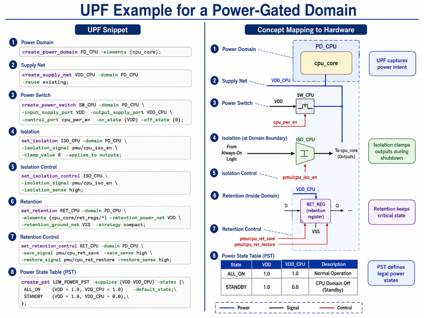
Isolation Cells
When a domain shuts down, its outputs become undefined. Isolation cells clamp these signals to known values to prevent corruption of active domains:
# UPF: Isolation strategy
set_isolation ISO_CPU \
  -domain PD_CPU \
  -isolation_power_net VDD \
  -isolation_ground_net VSS \
  -clamp_value 0 \
  -applies_to outputs \
  -name_prefix ISO_CPU_

set_isolation_control ISO_CPU \
  -domain PD_CPU \
  -isolation_signal {pmu/cpu_iso_en} \
  -isolation_sense high \
  -location parent

set_isolation ISO_GPU \
  -domain PD_GPU \
  -isolation_power_net VDD \
  -isolation_ground_net VSS \
  -clamp_value 0 \
  -applies_to outputs \
  -name_prefix ISO_GPU_

set_isolation_control ISO_GPU \
  -domain PD_GPU \
  -isolation_signal {pmu/gpu_iso_en} \
  -isolation_sense high \
  -location parent
Retention Registers
Critical state must survive power-down. Retention registers have a shadow latch powered by an always-on supply that captures state before shutdown and restores it on wakeup:
# UPF: Retention strategy
set_retention RET_CPU \
  -domain PD_CPU \
  -retention_power_net VDD \
  -retention_ground_net VSS

set_retention_control RET_CPU \
  -domain PD_CPU \
  -save_signal {pmu/cpu_save high} \
  -restore_signal {pmu/cpu_restore low} \
  -assert_count 1

# Specify which registers need retention
# (all flops in CPU domain by default, exclude non-critical)
set_retention_elements RET_CPU -elements {cpu_core/reg_file/* \
  cpu_core/pc_reg cpu_core/csr_bank/*} \
  -exclude_elements {cpu_core/debug_scratch/*}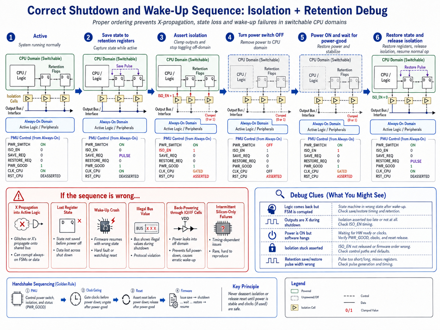
Power State Table
The power state table (PST) defines all legal power states and transitions. This is the contract between hardware and firmware — every state must be verified:
# UPF: Power state table
add_power_state PD_TOP.primary -state FULL_ON \
  {-supply_expr {power == FULL_ON}}
add_power_state PD_CPU.primary -state CPU_ON \
  {-supply_expr {power == FULL_ON}} \
  -state CPU_OFF {-supply_expr {power == OFF}}
add_power_state PD_GPU.primary -state GPU_ON \
  {-supply_expr {power == FULL_ON}} \
  -state GPU_OFF {-supply_expr {power == OFF}}

# Define legal combinations
create_pst LOW_POWER_PST \
  -supplies {VDD VDD_CPU VDD_GPU}

add_pst_state ALL_ON -pst LOW_POWER_PST \
  -state {FULL_ON FULL_ON FULL_ON}
add_pst_state CPU_ONLY -pst LOW_POWER_PST \
  -state {FULL_ON FULL_ON OFF}
add_pst_state GPU_ONLY -pst LOW_POWER_PST \
  -state {FULL_ON OFF FULL_ON}
add_pst_state STANDBY -pst LOW_POWER_PST \
  -state {FULL_ON OFF OFF}
3. Clock Gating
Clock gating is the single most effective dynamic power reduction technique at the logic level. By inserting integrated clock gating (ICG) cells, you eliminate switching on register banks that are not being written. Typical result: 20-40% dynamic power reduction.
- RTL-level clock gating — architects define enable conditions for register banks. Most effective because it captures design intent.
- Synthesis-level clock gating — Design Compiler or Genus automatically infers clock gating from enable conditions on flip-flops. Catches opportunities missed at RTL.
- Clock gating efficiency — measured as percentage of cycles where the gated clock is inactive. Target >60% for significant power savings.
# Design Compiler: Enable clock gating inference
set_clock_gating_style -sequential_cell latch \
  -positive_edge_logic {integrated} \
  -negative_edge_logic {integrated} \
  -minimum_bitwidth 4 \
  -max_fanout 64

# Synthesis with power optimization
compile_ultra -gate_clock -power

# Report clock gating results
report_clock_gating -nosplit
# Typical output: 85% of registers are clock-gated
# Clock gating efficiency: 62% average across all modes
4. Multi-Voltage Design (DVFS)
Dynamic Voltage and Frequency Scaling reduces dynamic power quadratically with voltage. Running at 0.6V instead of 0.8V gives a (0.6/0.8)2 = 56% dynamic power reduction at the cost of lower frequency. DVFS delivers 40-60% dynamic power reduction at lower performance modes.
Physical implementation requires voltage islands, level shifters at domain boundaries, and always-on buffers for control signals:
# ICC2: Multi-voltage physical implementation
# Create voltage areas
create_voltage_area -name VA_CPU \
  -power_domain PD_CPU \
  -coordinate {100 100 500 500}

create_voltage_area -name VA_GPU \
  -power_domain PD_GPU \
  -coordinate {550 100 950 500}

# Place level shifters at domain boundaries
set_app_options -name place.coarse.enable_lsb_placement -value true
set_app_options -name power.place_level_shifters -value near_source

# Insert always-on buffers for control signals
# crossing into shutdown domains
set_app_options -name power.insert_always_on_buffers -value true
insert_buffer -always_on [get_nets pmu/cpu_pwr_en]

# Power switch placement and routing
# (header-style switches along top of voltage area)
create_power_switch_array -power_switch SW_CPU \
  -direction horizontal -step 20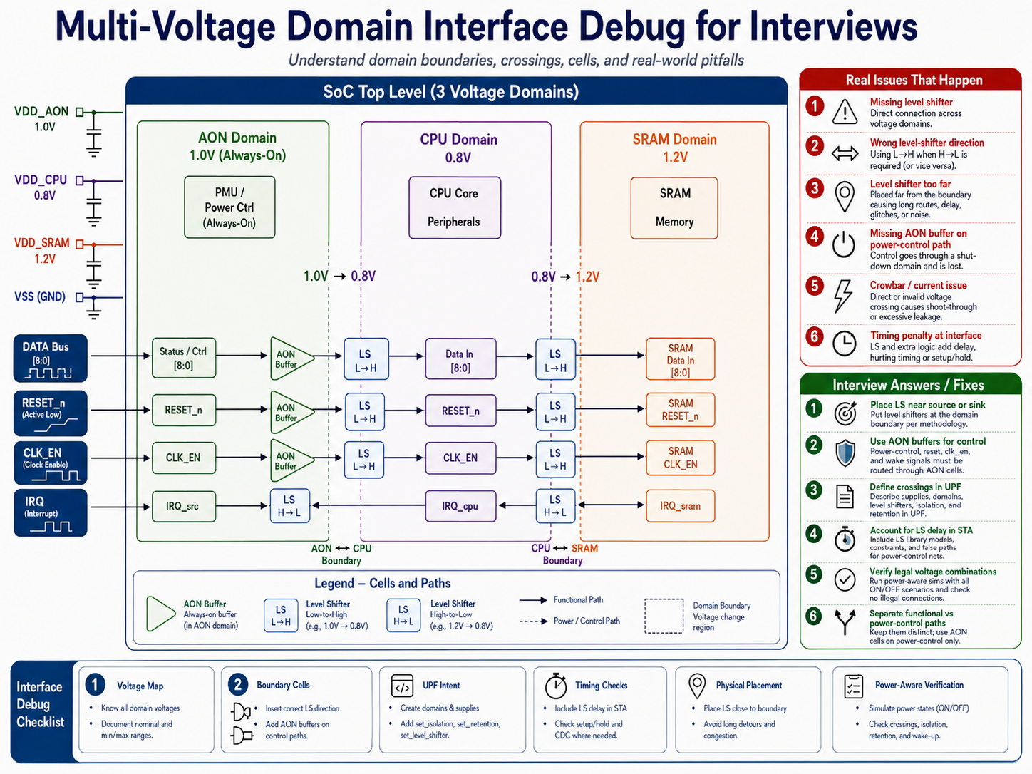
5. Operand Isolation and Data Gating
When a functional unit is idle, its inputs may still toggle due to upstream switching — causing unnecessary dynamic power in combinational logic. Operand isolation forces inputs to a constant value when the unit is inactive, eliminating spurious transitions:
# UPF: Operand isolation
set_isolation ISO_ALU_INPUTS \
  -domain PD_CPU \
  -elements {cpu_core/alu/operand_a cpu_core/alu/operand_b} \
  -isolation_power_net VDD_CPU \
  -clamp_value 0 \
  -applies_to inputs

set_isolation_control ISO_ALU_INPUTS \
  -domain PD_CPU \
  -isolation_signal {cpu_core/alu_enable} \
  -isolation_sense low \
  -location self
6. Memory Power Management
SRAMs dominate area and leakage on modern SoCs. Multi-mode memory controllers support graduated power states:
- Active — full speed read/write access
- Light sleep — periphery powered down, bitcells retain data, wakeup in 1-2 cycles. 40-60% leakage reduction.
- Deep sleep — voltage reduced to minimum retention level. 70-80% leakage reduction, wakeup in 5-10 cycles.
- Shutdown — complete power-off, data lost. 95%+ leakage reduction, requires full reload on wakeup.
# UPF: Memory power states
create_power_domain PD_L2_CACHE -elements {l2_cache}

add_power_state PD_L2_CACHE.primary \
  -state ACTIVE {-supply_expr {power == FULL_ON}} \
  -state LIGHT_SLEEP {-supply_expr {power == FULL_ON} \
    -simstate CORRUPT} \
  -state DEEP_SLEEP {-supply_expr {power == PARTIAL_ON}} \
  -state SHUTDOWN {-supply_expr {power == OFF}}
7. Substrate Biasing (Body Bias)
Adaptive body biasing shifts the threshold voltage dynamically:
- Forward Body Bias (FBB) — reduces Vt, increases speed, increases leakage. Apply in performance-critical active modes.
- Reverse Body Bias (RBB) — increases Vt, reduces leakage, reduces speed. Apply in idle/retention modes for additional leakage savings (20-40% on top of other techniques).
Implementation requires dedicated body bias voltage rails and on-chip bias generators. The physical design must route these additional supplies without impacting signal routing density.
8. Power-Aware CTS and Physical Design
The clock tree is the biggest single-net power consumer. Power-aware CTS techniques include:
- Clock mesh with selective density — denser mesh near high-frequency logic, sparser elsewhere
- Multi-source CTS — reduces buffer count and total capacitance versus single-source trees
- AOCV-aware clock tree — balance for variation, not just nominal skew — avoids over-buffering for margin
- Power-aware placement — co-locate high-activity cells to minimize switching capacitance on long nets
# ICC2: Power-aware CTS
set_app_options -name cts.common.power_aware_mode -value true
set_app_options -name clock_opt.power.effort -value high

# Limit clock buffer drive strengths to reduce power
set_lib_cell_purpose -exclude cts [get_lib_cells *BUF_X16*]
set_lib_cell_purpose -include cts [get_lib_cells *CKBUF_X4* *CKBUF_X8*]

# Power-aware placement optimization
set_app_options -name place_opt.flow.optimize_power -value true
place_opt -power

# Report clock power
report_power -clock_network
# Typical: clock network = 35% of dynamic power before opt
#          clock network = 22% after power-aware CTS
The Implementation Flow
Low-power design is not a single step — it is a methodology that spans the entire RTL-to-GDSII flow. Each stage builds on the previous:
| Stage | Key Activities | Tools |
|---|---|---|
| UPF Specification | Define power domains, switches, isolation, retention, PST | UPF 3.0, power architect |
| Power-Aware Synthesis | Clock gating inference, multi-Vt mapping, operand isolation | Design Compiler, Genus |
| Power-Aware Placement | Voltage area creation, switch placement, level shifter insertion | ICC2, Innovus |
| Power-Aware CTS | ICG-aware tree building, power-optimized buffering | ICC2 clock_opt |
| IR Drop Analysis | Static/dynamic IR drop, EM analysis, power grid reinforcement | RedHawk, Voltus |
| Power Signoff | Final power numbers, thermal map, power-state verification | PrimeTime PX, Voltus |
# ICC2: Complete power-aware PnR flow
# 1. Read UPF
load_upf ./scripts/top_power_intent.upf
commit_upf

# 2. Create power grid
create_pg_ring_pattern ring_pattern -horizontal_layer M9 \
  -vertical_layer M10 -horizontal_width 2.0 \
  -vertical_width 2.0 -horizontal_spacing 1.0 \
  -vertical_spacing 1.0
create_pg_mesh_pattern mesh_pattern -layers {M7 M8} \
  -widths {0.8 0.8} -pitches {20 20}

set_pg_strategy core_ring -pattern ring_pattern \
  -core -extension {{stop:outermost_ring}}
set_pg_strategy core_mesh -pattern mesh_pattern \
  -core -extension {{stop:outermost_ring}}

compile_pg -strategies {core_ring core_mesh}

# 3. Place power switches
create_power_switch_array -power_switch SW_CPU \
  -direction horizontal -step 20 -offset 5
place_power_switches

# 4. Run power-aware optimization
place_opt -power
clock_opt -power
route_auto
route_opt -power

# 5. Analyze IR drop
analyze_power_plan -nets {VDD VSS}
report_power -scenarios {active standby retention}

# 6. Export for signoff
write_parasitics -format spef -output ./output/power_signoff.spef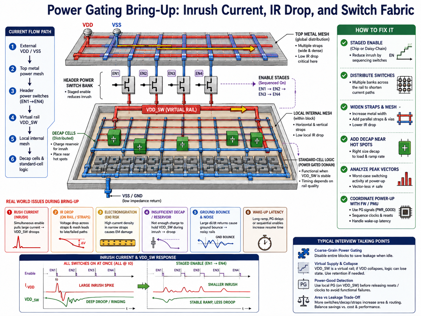
Real Numbers: Power Reduction by Technique
From our recent tapeouts at 7nm and 5nm, here are the actual power reduction percentages achieved at each stage. These numbers are from production silicon, not estimates:
| Technique | Power Reduction | Component Affected | Implementation Cost |
|---|---|---|---|
| Clock gating (synthesis + RTL) | 20-40% | Dynamic | Low — mostly automated |
| Multi-Vt swap (HVT dominant) | 30-50% | Leakage | Low — tool-driven, minor timing impact |
| Power gating (full shutdown) | 90%+ | Leakage (domain) | Medium — UPF, switches, isolation, retention |
| DVFS (0.8V to 0.6V scaling) | 40-60% | Dynamic | Medium — voltage regulators, level shifters |
| Memory light sleep | 40-60% | Leakage (SRAM) | Low — memory compiler support |
| Memory deep sleep | 70-80% | Leakage (SRAM) | Low-Medium — longer wakeup latency |
| Operand isolation | 5-15% | Dynamic (datapath) | Low — synthesis option |
| Power-aware CTS | 10-20% | Dynamic (clock) | Low — tool options during CTS |
| Reverse body bias (idle) | 20-40% | Leakage | High — bias generators, routing |
Cumulative impact on a representative 5nm mobile SoC (application processor, 4-core CPU + GPU + NPU):
- Baseline (no power optimization) — 8.2W total at peak, 1.8W idle
- After clock gating — 5.7W peak (-30%), 1.8W idle (no change)
- After multi-Vt swap — 5.7W peak, 1.1W idle (-39% leakage)
- After power gating (3 of 4 CPU cores idle) — 3.8W typical, 0.3W standby
- After DVFS (low-perf mode at 0.6V) — 1.9W typical at 50% performance
- Final silicon with all techniques — 4.1W sustained typical, 0.25W deep standby
Power Verification: Getting UPF Right
A power intent bug is a silicon bug. Unlike timing violations that can sometimes be fixed with frequency binning, a missing isolation cell or incorrect retention mapping causes hard functional failure. Power-aware verification must cover:
- Structural checks — every signal crossing a power boundary has an appropriate isolation cell, level shifter, or always-on buffer
- Sequential checks — retention save/restore sequences are correct, power-up sequences do not violate timing
- State coverage — every PST state has been simulated, every transition has been exercised
- Corruption propagation — when a domain shuts down, no X-propagation reaches active logic
# Power-aware simulation with UPF
# (Synopsys VCS example)
vcs -power=top_power_intent.upf \
    -power_top tb/dut \
    -assert enable_diag \
    +power+shutdown_check \
    +power+isolation_check \
    +power+retention_check \
    -f filelist.f

# Static power verification (Synopsys MVtools / Cadence CLP)
# Check all boundary signals have isolation
verify_pg_connectivity
check_lp_rules -all
check_mv_design -power_domain_crossing
report_isolation_cells -missing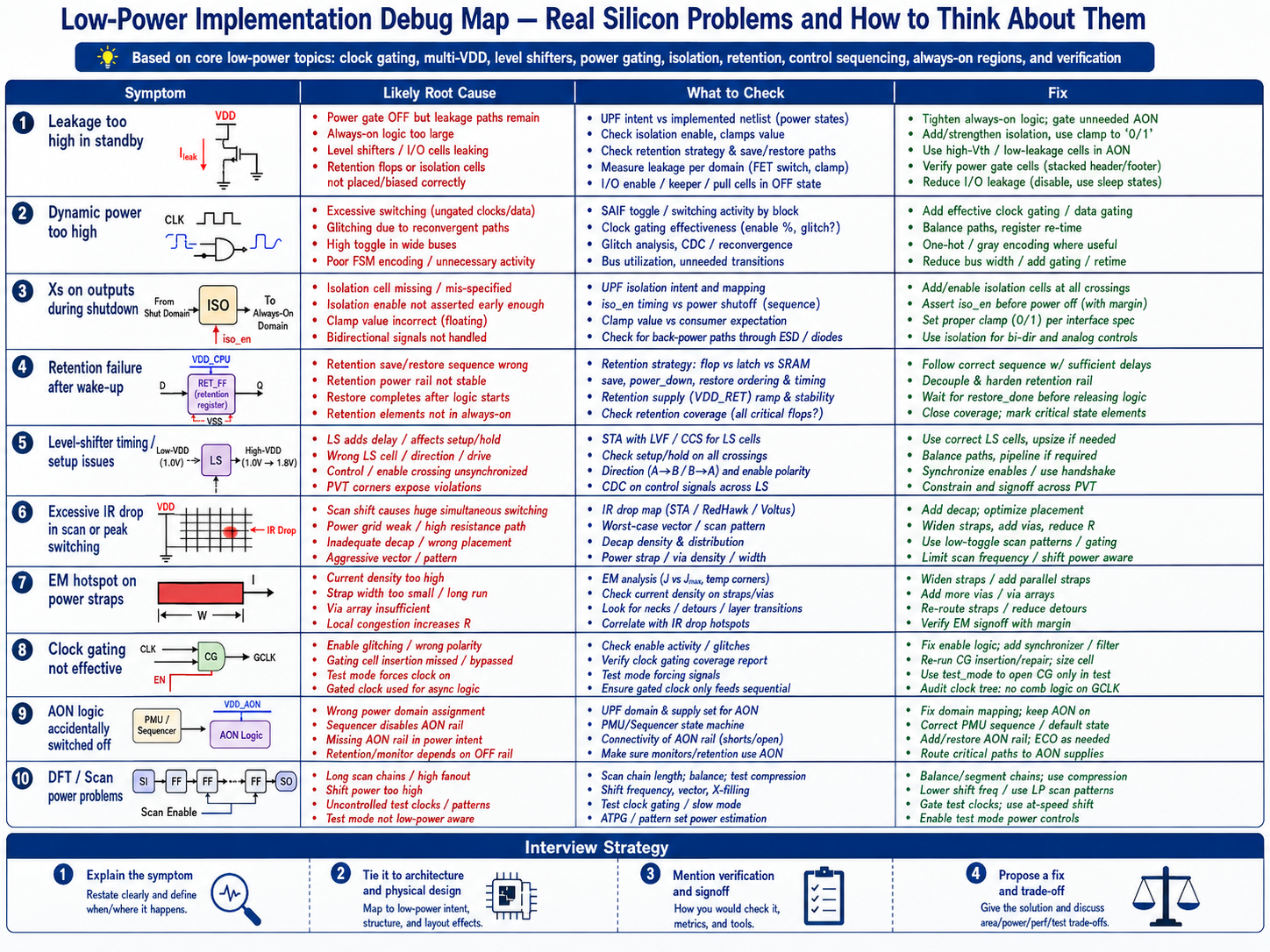
IR Drop: The Hidden Power Failure Mode
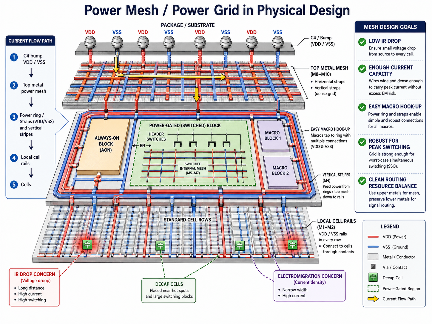
IR drop does not waste power — it prevents delivery of the power you need. Dynamic IR drop during high-activity events (scan shift, burst workloads) can cause functional failures that only appear in silicon. Our IR drop methodology:
- Static IR drop — DC analysis with average current per instance. Target: <5% VDD drop at any point.
- Dynamic IR drop — transient analysis with realistic switching vectors. Target: <8% VDD drop for worst-case events.
- EM (Electromigration) — current density must not exceed foundry limits for 10-year lifetime. Check all power and signal nets.
# RedHawk/Voltus: IR drop analysis flow
# 1. Import design and power grid
import_design -def ./output/final.def \
  -lef {tech.lef std_cell.lef}
import_pg_library

# 2. Map switching activity
read_activity_file -format fsdb -file ./sim/power_vectors.fsdb
set_power_pads -net VDD -file vdd_pads.txt
set_power_pads -net VSS -file vss_pads.txt

# 3. Run dynamic IR analysis
set_analysis_mode -method dynamic
run_ir_analysis -duration 10ns -time_step 0.1ns

# 4. Report and fix
report_ir_drop -threshold 0.040 -net VDD
# Fix: add decap cells in hotspot regions
# Fix: widen power stripes in high-current zones
# Fix: add via stacks between power layers
Practical Lessons from Tapeouts
After multiple low-power tapeouts at 7nm and 5nm, here are the lessons that do not appear in textbooks:
- Start UPF at architecture, not implementation — retrofitting power domains is 10x more expensive than designing them in from the start
- Budget 15-20% area overhead for power management — switches, isolation, retention, always-on logic, and power grid reinforcement all take area
- Rush current is your biggest power gating risk — a domain powering up simultaneously draws massive current. Use daisy-chain switch enable with staggered turn-on.
- Retention is expensive — use it sparingly — each retention register costs 40-60% more area than a standard flop. Only retain architectural state (register file, PC, critical CSRs). Let caches reload from memory.
- Clock gating efficiency degrades with test modes — scan chains force all gating open. Budget power for test mode separately.
- Verify wakeup latency meets interrupt response requirements — a power-gated domain that takes 50us to wake up cannot service a 10us interrupt deadline
- IR drop and power gating interact — the rush current from wakeup is the worst-case dynamic IR drop event. Simulate it explicitly.
- Multi-Vt swap at signoff, not during implementation — let timing close first with SVT/LVT, then swap non-critical paths to HVT. Doing it earlier causes unnecessary timing iterations.
Closing Thoughts
Low power design at advanced nodes is a full-stack discipline. It starts at architecture (what can be power-gated?), flows through RTL (clock gating, data gating), is formalized in UPF (power domains, isolation, retention), and is implemented through power-aware physical design (multi-Vt, power-aware CTS, DVFS, IR drop closure). No single technique is sufficient — you need the entire stack working together.
The teams that ship power-efficient silicon are the ones that treat power as a first-class design constraint from day one, specify UPF alongside RTL, verify power states alongside function, and have methodology that spans from architecture decisions through physical signoff. The tools are mature. The techniques are proven. What separates success from failure is rigorous application of methodology and early investment in power architecture.
Power will continue to be the defining constraint of semiconductor design for the foreseeable future. The teams and companies that master it will build the chips that define the next generation of mobile, edge AI, and data center computing.