Large language models look elegant at the mathematical level: tokens become vectors, vectors move through repeated transformer layers, and the model produces probabilities for the next token. In silicon, however, those equations turn into a much harder engineering problem.
An LLM accelerator must perform enormous amounts of matrix and tensor computation while moving weights, activations, and key-value (KV) cache data through a limited amount of on-chip memory, interconnect, package bandwidth, power, and routing resources. This is where architecture meets physical design.
This article builds a practical physical-design mental model for the kinds of issues an LLM accelerator creates — from transformer math all the way down to congestion, IR drop, and thermal hotspots.
1. From Transformer Math to a Hardware Workload
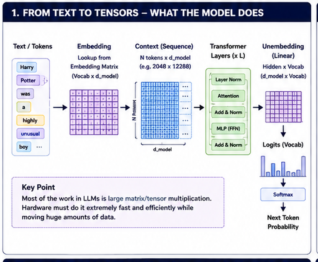
The transformer starts with text, but the hardware very quickly sees numbers. A simplified flow is:
Text
  ↓
Tokens
  ↓
Embedding vectors
  ↓
Repeated transformer layers
  ├─ Attention (Q, K, V matrix ops)
  └─ Feed-forward / MLP
  ↓
Final hidden state
  ↓
Unembedding / output projection
  ↓
Logits → Softmax → Next-token probability
The embedding lookup is largely a memory-access problem. Once the representation enters the transformer layers, a large fraction of the work becomes matrix multiplication, tensor arithmetic, reductions, normalization, and data movement.
From the chip designer's point of view, two things dominate:
- Compute throughput — how many multiply-accumulate operations per second
- Data movement efficiency — getting weights and activations to compute without stalling
A matrix engine can be extremely fast, but it does not help if it is continuously waiting for weights or activations.
2. A Simplified LLM Accelerator Architecture
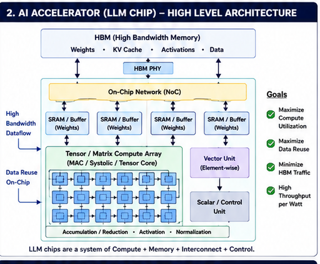
A useful conceptual architecture contains:
- Tensor / matrix compute arrays — MAC units, systolic arrays, or tensor cores for multiply-accumulate-heavy work
- On-chip SRAM — for weights, activations, partial results, and frequently reused data
- HBM / external DRAM — for model state that cannot fit on-chip
- Network-on-Chip (NoC) — to move data between compute, memory, and I/O
- Vector/scalar units — for element-wise operations, reductions, activation functions, and control
- Clock, reset, scan, and power-management infrastructure
The architectural goal is simple to state:
Keep expensive compute units busy while minimizing data movement.
But physically this immediately becomes complicated. Large SRAM macros consume area. Wide buses consume routing tracks. High-bandwidth interfaces constrain floorplanning. Large compute arrays create high switching activity and current demand. All of these effects interact with timing.
3. Prefill vs Decode — Two Very Different Workloads
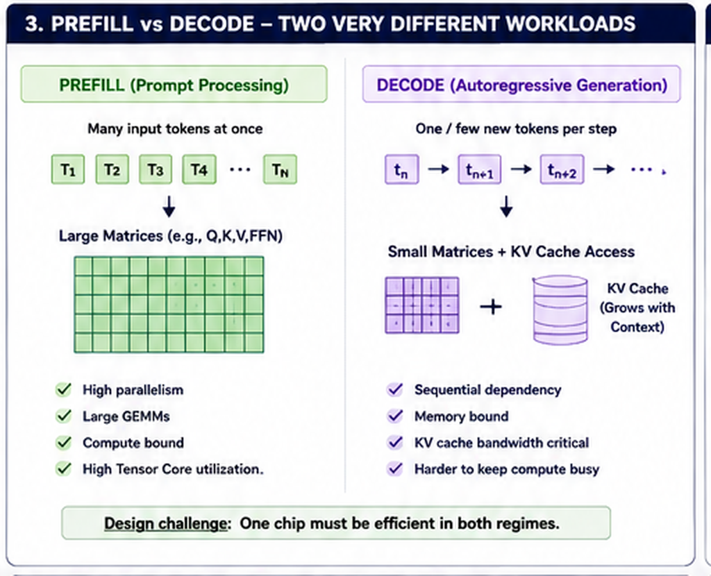
LLM inference is not one uniform workload. The same chip must handle two fundamentally different operating regimes.
Prefill (Prompt Processing)
During prefill, many prompt tokens are processed together. This gives:
- Large matrix operations — high parallelism, large GEMMs
- Compute-bound behavior — tensor cores stay highly utilized
- Good data reuse — weights amortized across many tokens
Decode (Autoregressive Generation)
During decode, the model generates one or a few new tokens at a time. Now the chip repeatedly needs to access model weights, the growing KV cache, and the latest hidden representation. The workload becomes:
- Memory-bandwidth bound — small matrix ops, large memory reads
- Sequential dependency — each token depends on the previous
- KV cache bandwidth critical — cache grows with context length
- Harder to keep compute busy — tensor cores often stall waiting for data
Design challenge: one chip must be efficient in both regimes. This affects memory hierarchy, NoC design, buffer sizing, compute-array shape, and ultimately the floorplan.
4. Physical Design Challenges in AI Chips
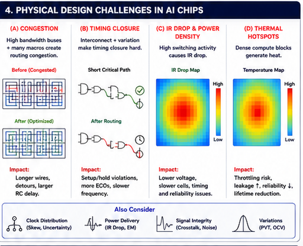
4.1 Routing Congestion
AI accelerators contain many repeated processing elements, wide data buses, large SRAM macros, high-bandwidth NoC links, and interfaces to HBM PHYs. All compete for limited routing resources.
If the floorplan forces too many buses through the same area, routing detours appear:
Congestion
   ↓
Longer routes
   ↓
Higher RC delay
   ↓
Setup violations
   ↓
More ECOs, slower frequency
Physical designers respond by moving or rotating macros, opening routing channels, reducing placement density, assigning higher metal layers to long buses, and coordinating with architecture when the physical structure itself is the bottleneck.
Floorplanning is often the first timing optimization.
4.2 Timing Closure
AI chips often have aggressive frequency targets and long interconnect between compute, SRAM, NoC, and control logic. Path delay is not only gate delay:
Total path delay = cell delay + wire RC + coupling + clock uncertainty + PVT variationOn advanced nodes, the wire can be as important as the logic. One of the most difficult loops is:
Timing violation
    ↓
Upsize cell / add buffer
    ↓
More area + capacitance
    ↓
More congestion
    ↓
Longer wires
    ↓
Timing gets worse
This is why timing closure cannot be treated as a sequence of isolated gate fixes. The physical context matters — and Multi-Mode Multi-Corner (MMMC) analysis becomes essential to converge across the full operating space.
4.3 IR Drop and Power Density
AI compute arrays have very high switching activity because many MAC units operate simultaneously. Combined with wide buses, large clock networks, high frequency, and large SRAM structures, this creates substantial power density.
The power grid has resistance. When compute activity increases:
Current ↑
   ↓
IR drop ↑
   ↓
Local VDD ↓
   ↓
Cell delay ↑
   ↓
Timing margin ↓
This means power-integrity analysis and STA are not independent activities. A path that closes under ideal voltage may fail in a region suffering dynamic voltage droop.
4.4 Thermal Hotspots
Dense compute arrays create localized heat. Higher temperature causes increased leakage, timing shifts, reliability degradation, and additional power-grid stress. The feedback loop can become self-reinforcing:
Activity ↑ → Power ↑ → Temperature ↑ → Leakage ↑ → Power ↑ (again)Thermal-aware floorplanning is critical for large AI accelerators to avoid throttling risk and lifetime reduction.
5. How These Issues Impact Timing and Power
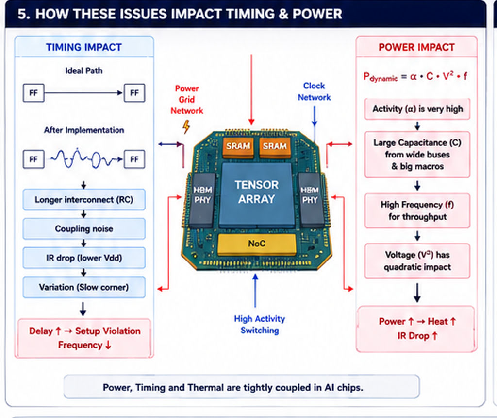
Dynamic power follows the relationship:
P_dynamic = α · C · V² · f

where:
  α = switching activity (very high in tensor arrays)
  C = switched capacitance (large buses + big macros)
  V = supply voltage (quadratic impact)
  f = frequency (high for throughput)
Power, timing, and thermal behavior are tightly coupled in AI chips. A stronger power grid improves IR drop and electromigration, but wider power metal consumes routing resources — potentially increasing congestion. This is the fundamental tradeoff that physical design must navigate.
Electromigration
High current density creates electromigration risk in power straps, vias, clock networks, and local high-current structures. Fixes include wider metal, more vias, additional straps, and better current spreading — but all of these compete for routing resources.
Clock Distribution
A large tensor engine may contain millions of sequential elements. The clock network must control skew, insertion delay, OCV sensitivity, transition quality, clock power, and routing congestion — all simultaneously. A CTS change can affect timing, power, IR drop, and congestion at once.
6. Physical Design Solutions and Best Practices
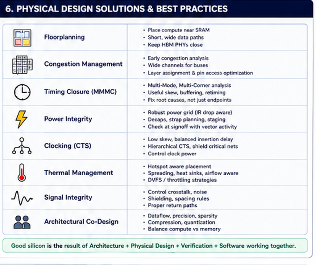
Floorplanning
- Place compute near SRAM — minimize data path latency
- Short, wide data paths — reduce RC delay on critical buses
- Keep HBM PHYs close — bandwidth-critical interfaces need minimal routing distance
- Avoid power concentration — spread high-activity blocks to prevent thermal hotspots
Congestion Management
- Early congestion analysis — detect problems before detailed routing
- Wide channels for buses — reserve routing capacity for high-bandwidth data paths
- Layer assignment and pin access optimization — use higher metals for long runs
- Restructure networks when physical topology creates bottlenecks
Timing Closure (MMMC)
- Multi-Mode Multi-Corner from early stages — don't bolt it on at signoff
- Useful skew, buffering, retiming — intentional clock scheduling
- Fix root causes, not just endpoints — placement quality before brute-force upsizing
- ECO awareness — batch fixes by region, track WNS/TNS convergence
Power Integrity
- Robust power grid — IR-drop-aware strap and via planning
- Decaps and staging — manage dynamic current transients
- Check at signoff with vector activity — static analysis alone misses dynamic droop
- Consider DVFS and power gating where architecture permits
Thermal Management
- Hotspot-aware placement — spread high-power blocks
- Heat sinks and airflow awareness — coordinate with package assumptions
- DVFS / throttling strategies — graceful degradation under thermal stress
Signal Integrity
- Control crosstalk and noise — spacing, shielding, layer assignment
- Proper return paths — clean reference planes
- SI-aware STA — account for coupling in timing analysis
Architectural Co-Design
Some problems cannot be solved by physical implementation alone. When an SRAM is simply too far from compute, a NoC requires too much bandwidth through one region, or a clock target is unrealistic for the topology — the best "physical-design fix" is architectural feedback.
Good silicon is the result of Architecture + Physical Design + Verification + Software working together.
7. Why AI Silicon Is Harder Than Traditional Workloads
A chip takes years to architecture, implement, verify, fabricate, and deploy. AI models change much faster. This creates a difficult balance:
| Approach | Benefit | Risk |
|---|---|---|
| High specialization | Excellent efficiency today | May become obsolete with next model architecture |
| High flexibility | Supports evolving workloads | Wastes power and area on generality |
An AI accelerator must balance compute throughput, memory capacity, bandwidth, on-chip data reuse, interconnect, PPA, implementation feasibility, and flexibility for evolving models. Full-stack co-design is essential.
8. The Physical-Design View of PPA
Physical design is ultimately about finding a workable balance among Performance, Power, and Area:
- Upsizing a cell may improve delay but increase power and capacitance
- Adding buffers may fix timing but increase area and congestion
- Wider spacing improves signal integrity but increases wirelength
- More power straps improve IR drop but consume routing resources
- Larger SRAM reduces external memory traffic but makes floorplanning harder
- Higher frequency improves throughput but increases dynamic power and timing pressure
There is rarely a single perfect answer. The best AI silicon is the design in which compute, memory, interconnect, timing, power, thermal behavior, package assumptions, and physical implementation work together as one system.
Conclusion
The mathematics of an LLM may be expressed as embeddings, attention, matrix multiplication, and probability distributions. But the silicon implementation has to deal with wires, resistance, capacitance, voltage drop, clocks, variation, heat, finite routing resources, and physical area.
Architecture defines what the chip wants to do. Physical design determines whether it can actually do it at the required performance, power, area, and reliability.
For LLM accelerators, the hardest problems sit at the boundaries: compute vs memory, architecture vs floorplan, power vs timing, clock vs variation, bandwidth vs congestion, performance vs thermal limits. Mastering these boundaries is what separates good AI silicon from great AI silicon.